 alt Hacker News
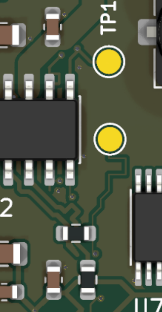
The PCB looks super weird, what is going on here?
https://files.catbox.moe/nijoin.png
https://files.catbox.moe/suazr4.png
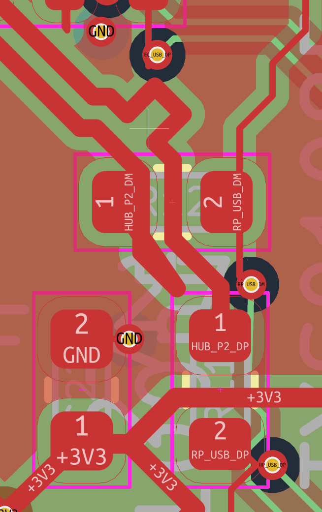
They sort of look sensible until you look closer and then the whole board is fever dream autorouting.
Replies
abijahkaj • yesterday at 9:20 PM
yeah it's raw output from the router i'm coding without a trace smoothing pass yet, so it draws ugly jagged steps. looks bad to a human layout engineer, no argument there. either way it won't stop it from working, the electrons don't care how ugly the bend is at 2 MHz. just want to see if it boots when the jlcpcb parcel lands.
edit: idk why my comments are being [flagged], i've written to hn but the issue is apparently still there
they answered with AI and got flagged for being AI. You can turn on showdead in settings to see it but there's nothing of value in their comment really.