People have been doing this for a long time, but it feels a little too purist to me.
The components will still be the same, so you'll still need some kind of pick-n-place functionality to make anything, so why not just have another print head for making the traces / doing the PnP?
The head could lay copper wire/foil tape for conductors and do standard PnP from trays / reels of components, which you'll need either way.
It would be a little more geometrically limited than what this post imagines, but it would have the upside that it would actually work today and with most real electronics applications, unlike the low performance conductors made via conductive polymers as the OP's process imagines.
Replies
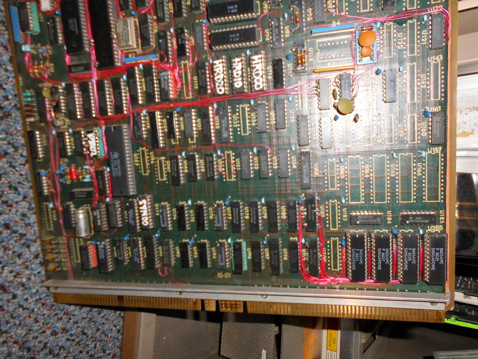
This reminds me a bit of Multiwire, a somewhat unusual circuit manufacturing technique from the 1980s. A machine laid down wires and then encased them in resin. The best info I can find is this slide deck:
https://www.swtest.org/swtw_library/2013proc/PDF/SWTW13-22.p...
I believe this technique was used in the Three Rivers PERQ computers. Here is an image of one of their PCBs https://blogger.googleusercontent.com/img/b/R29vZ2xl/AVvXsEg...
A PnP placing the components upside down onto a surface printed by another head would be interesting. You could align the heights of the resting surfaces to optimise pads needing to be connected being on the same plane. I'd still want to lay copper but if you had the ability to squirt a little solder paste from (yet another) head, you could stack everything with wire connections into a very 3d circuit.
If the base material was thermally conductive you could have a heatsink block with the circuit embedded in it.
I think the "printegrated circuits" approach is roughly the right level of abstraction.
3D Printing the PCB itself is pretty much impossible for any non-trivial application. Doing multi-layer PCBs with 0.20mm wide traces, spaced 0.20mm apart? Forget it, not happening - and requirements like those are standard for hobbyist-level chips like the RP2040 these days.
And if you're not printing your own PCB, what's left is module-level assembly and connectivity. In other words, just printing a bunch of wires.
For this in 2D, see Sam's thesis, 6.3.3 (p. 86, CNC wire plotting). 3D would add a lot of challenges.
> The head could lay copper wire/foil tape for conductors
Sounds awesome, but this is an extremely hard problem to solve. You can't simply lay down wire or foil into arbitrary shapes on 3D surfaces.